










Published by MEAXPERT | Cost-Effective Precision Measurement Solutions
Introduction: When Microns Matter, Measurement Matters More
Driven by the rapid growth of AI, high-performance computing, and advanced electronics, the semiconductor industry continues to move toward smaller features, higher integration, and more complex manufacturing processes. From semiconductor wafers and advanced packaging components to precision PCBs and semiconductor manufacturing equipment, dimensional tolerances are becoming more demanding. In many applications, even micrometer-level deviations can affect assembly accuracy, process stability, product performance, and manufacturing yield.
This creates a critical challenge for manufacturers: How can measurement remain fast, accurate, and consistent as feature sizes shrink and inspection volumes increase?
Vision Measuring Machines (VMMs) provide an effective non-contact solution for many of these applications. By combining high-resolution optical imaging, precision motion control, automated measurement software, and programmable inspection routines, VMMs can help manufacturers improve both measurement efficiency and quality control. This article explores two common semiconductor measurement challenges and explains how vision measurement technology can support high-precision inspection in semiconductor and related manufacturing applications.

- Flip-Chip & Micro-Bump Measurement: High-Density Micro-Feature Inspection
Advanced semiconductor packaging relies heavily on dense interconnection structures to support compact, high-performance chip designs. In flip-chip packaging, the dimensions and positions of micro-bump arrays directly influence alignment accuracy and electrical connection reliability, making consistent dimensional and positional inspection essential for stable packaging yields.
Typical micro-bump and flip-chip inspection tasks cover a broad set of dimensional and positional verifications:
- X and Y coordinate deviation relative to reference datums
- Bump diameter, feature spacing, and pitch consistency
- Component alignment accuracy and positional tolerance
- Surface dimensional characteristics of micro-scale packaging structures
Modern flip-chip designs often incorporate hundreds of densely packed micro-bumps. Traditional manual and contact inspection methods struggle to balance throughput, repeatability, and precision, creating several common inspection challenges for high-volume packaging lines.
Challenge 1: High-Density Features Increase Inspection Complexity
Semiconductor micro-bump arrays consist of large quantities of repeated micro-features that require multi-point geometric verification. Manual inspection requires extensive repetitive work, which increases cycle time and introduces variability between operators. For production environments, inspection systems need to automate feature recognition, streamline multi-point measurement, and reduce manual intervention to maintain stable throughput and consistent results across batches.
Automated vision measurement can help address these challenges by combining CNC motion control, image processing, and programmed inspection routines. The technology efficiently measures large numbers of repeated features through standardized automated workflows, supporting more consistent and productive batch inspection.
Challenge 2: Variable Surface Heights Require Adaptive Focus Control
Chip surfaces, micro-bump structures, and packaging substrates often present surface height variations across the workpiece. Conventional optical measurement workflows require frequent manual focusing adjustments, which slow down inspection cycles and limit automation potential.
Depending on the configuration and application requirements, vision measurement systems can be equipped with automatic focusing and programmable Z-axis measurement functions to improve measurement efficiency on components with varying surface heights. These adaptive features reduce manual adjustments and support continuous and highly automated inspection workflows for packaging components with uneven surface profiles.
Challenge 3: Delicate Component Structures Are Poorly Suited for Contact Inspection
Many semiconductor and electronic components feature delicate surfaces, fine structures, or thin geometries that can make contact measurement unsuitable for certain inspection tasks. Mechanical probing may introduce localized contact forces that could affect delicate surfaces or sensitive structures.
Non-contact optical measurement eliminates direct physical contact with workpieces. Vision measurement systems capture geometric data through high-resolution imaging and software-based feature analysis, which helps reduce the risk of damage during inspection. This method is well suited for semiconductor wafers, microchips, advanced packaging structures, precision substrates, and micro-electronic components.
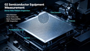
- Semiconductor Equipment Measurement: Dense Hole Pattern Inspection
Growing demand for semiconductor devices has raised quality requirements for manufacturing equipment and precision mechanical components. Process tools such as etching and deposition systems rely on high-precision parts with structured surface patterns, where feature position and dimension directly influence process uniformity and wafer processing stability.
Showerhead components, a common example in semiconductor processing equipment, feature dense arrays of gas distribution holes. Accurate inspection of these features helps verify conformity to design requirements, supporting consistent gas distribution and stable process performance. Typical measurement requirements include:
- Hole diameter tolerance
- Hole positional accuracy and X/Y coordinate consistency
- Inter-hole distance, pitch uniformity, and pattern accuracy
- Component flatness and other surface-related characteristics
Challenge 1: High-Density Hole Patterns Reduce Manual Inspection Efficiency
Individual equipment components can contain hundreds of holes distributed across the surface, sometimes in irregular patterns. Manual inspection of each feature is labor-intensive and prone to human error, making it difficult to maintain standardized results across production batches.
MEAXPERT CNC vision measurement systems can help improve the efficiency and consistency of this inspection process. Once configured, automated inspection programs guide the system through positioning, image acquisition, edge detection, dimensional calculation, and tolerance comparison. The workflow minimizes repetitive manual work and delivers traceable, repeatable inspection data for quality validation and batch comparison.
Challenge 2: Inspection Throughput Must Align With Production Capacity
In semiconductor equipment manufacturing, low inspection throughput can restrict overall production capacity. As batch sizes expand, manufacturers require measurement solutions capable of handling increasing inspection volumes without compromising accuracy.
Modern vision measurement platforms integrate programmable motion control, high-speed image capture, automated feature recognition, and optimized measurement paths. These capabilities support efficient batch inspection workflows and shorter measurement cycles compared with manual methods, helping manufacturers improve quality control efficiency for high-volume precision component production.
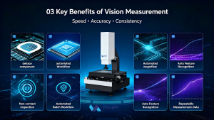
- Key Benefits of Vision Measurement for Semiconductor Applications
Semiconductor manufacturing requires a careful balance between measurement precision and inspection productivity. Effective measurement systems must deliver reliable accuracy while supporting production throughput and consistent inspection processes. Vision measurement technology provides an effective solution for a wide range of semiconductor and precision electronic inspection applications, with several practical advantages for modern manufacturing environments.
Non-Contact Inspection for Delicate Precision Parts
Optical, non-contact measurement avoids mechanical interaction with component surfaces. This approach supports quality verification for thin substrates, sensitive micro-structures, and fine-pitch electronic components, helping reduce the risk of surface damage or structural alteration during inspection.
Automated Workflows Improve Batch Efficiency
CNC-enabled programmable measurement allows operators to reuse standardized inspection routines across multiple workpieces. Automated execution reduces manual operation variability and supports more consistent throughput in batch production scenarios.
Automated Feature Recognition for Complex Geometries
Advanced measurement software supports automatic edge detection and geometric analysis for common features, including holes, circles, lines, slots, distances, angles, and coordinate positions. This functionality simplifies inspection for repetitive micro-feature arrays and complex patterned components typical in semiconductor packaging and equipment parts.
Enhanced Process Repeatability and Data Consistency
Manual measurement results often vary based on operator technique and experience. Programmed vision inspection applies consistent motion paths, lighting parameters, and calculation logic across all samples. This improves result repeatability, data comparability, and overall quality control reliability for high-precision manufacturing processes.
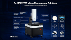
- MEAXPERT Vision Measurement Solutions for Semiconductor Applications
MEAXPERT provides cost-effective precision measurement solutions for advanced manufacturing applications. Our Vision Measuring Machines can support quality inspection for a variety of high-precision components, including:
- Semiconductor wafers, chips, and advanced packaging components
- Precision PCBs, substrates, and micro-electronic parts
- Precision components for semiconductor manufacturing equipment
- High-density hole pattern and micro-feature batch inspection
- Precision mechanical components, mold tooling, and industrial precision parts
Depending on the application, MEAXPERT systems can be configured with capabilities such as CNC automatic measurement, high-resolution cameras, precision motion systems, programmable lighting, automatic focusing functions, and advanced measurement software. These configurable features help manufacturers build targeted measurement workflows aligned with specific accuracy requirements, feature complexity, throughput goals, and automation levels.
By selecting the appropriate system configuration, manufacturers can balance measurement performance, inspection efficiency, investment cost, and long-term production requirements.
- Driving Process Improvement Through Reliable Measurement Data
Measurement continues to evolve from a standalone final inspection step to an integrated part of process control. Accurate and reliable measurement data is becoming increasingly important for process monitoring and quality improvement. Consistent dimensional verification helps manufacturers identify process deviations early, support process adjustments, reduce the risk of defects, and improve manufacturing consistency.
As semiconductor features shrink and process architectures grow more complex, stable, repeatable, and efficient precision measurement becomes essential for maintaining competitive manufacturing quality.
Conclusion: Precision Measurement for a More Demanding Semiconductor Industry
In semiconductor manufacturing, small dimensional deviations can have a significant impact on product performance, assembly quality, and manufacturing consistency. From high-density micro-bump structures in advanced packaging to complex hole patterns in semiconductor equipment components, manufacturers face growing pressure to improve both inspection accuracy and measurement efficiency.
For many of these applications, Vision Measuring Machines offer important advantages, including non-contact measurement for delicate or sensitive surfaces, automated routines for high-density feature inspection, reliable dimensional and positional verification, improved repeatability through programmed workflows, and higher throughput for batch production.
By combining optical imaging, precision motion control, and advanced measurement software, vision measurement technology can help manufacturers make inspection faster, more consistent, and easier to integrate into modern quality-control workflows.
MEAXPERT provides cost-effective Vision Measuring Machine solutions designed around different workpiece sizes, measurement requirements, and production needs.
Looking for a suitable vision measurement solution for semiconductor or precision electronic components? Contact MEAXPERT to discuss your application and measurement requirements.